|
|
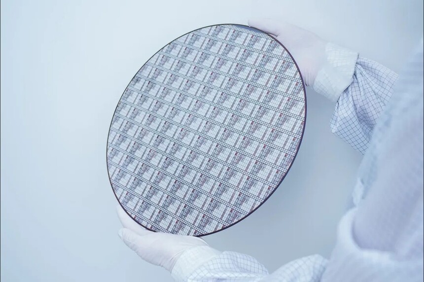
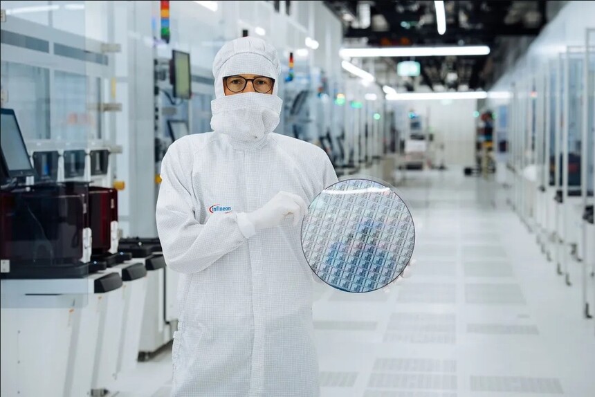
Infineon realizes world's first 300 mm GaN power semiconductor technologyInfineon Technologies AG announced today that it has successfully developed the world's first 300mm gallium nitride (GaN) power semiconductor wafer technology. Infineon is the first company in the world to master this breakthrough technology in an existing and scalable mass production environment. This breakthrough will greatly promote the development of the GaN power semiconductor market. Compared with 200mm wafers, 300mm wafer chip production is not only technically more advanced, but also because of the expansion of wafer diameter, the number of chips on each wafer has increased by 2.3 times, and the efficiency has also been significantly improved.
GaN-based power semiconductors are rapidly gaining popularity in industrial, automotive, consumer, computing and communication applications, including AI system power supplies, solar inverters, chargers and adapters, and motor control systems. Advanced GaN manufacturing processes can improve device performance and bring many benefits to end-customer applications, including higher efficiency, smaller size, lighter weight and lower total cost. In addition, with scalability, the 300mm manufacturing process has extremely high stability in customer supply. Infineon has successfully produced 300mm GaN wafers in its power semiconductor wafer fab in Villach, Austria, using an integrated pilot line of existing 300mm silicon production equipment. Infineon is leveraging its existing mature production capacity of 300mm silicon and 200mm GaN, and will further expand GaN production capacity based on market demand. With 300mm GaN process technology, Infineon will drive the continuous growth of the GaN market. It is estimated that the GaN market will reach billions of dollars by the end of 2030.
This groundbreaking technological achievement highlights Infineon's position as a global leader in power systems and IoT semiconductors. Infineon is building more cost-effective and valuable products that meet the full range of customer system needs through the deployment of 300mm GaN technology to strengthen existing solutions and enable new solutions and application areas. In November 2024, Infineon will present the first 300mm GaN wafers to the public at the Munich Electronics Show (electronica). Since the manufacturing processes of GaN and silicon are very similar, a major advantage of 300mm GaN technology is that it can use existing 300mm silicon manufacturing equipment. Infineon's existing high-volume 300mm silicon production lines are very suitable for pilot production of reliable GaN technology, which not only speeds up the implementation, but also enables efficient use of capital. The full-scale production of 300mm GaN will help achieve the cost of GaN and silicon at the same RDS(on) level, which means that the cost of silicon and GaN products of the same level will be equal. 300mm GaN is another milestone in Infineon's strategic innovation leadership and will help Infineon achieve its low-carbon and digitalization mission. |


